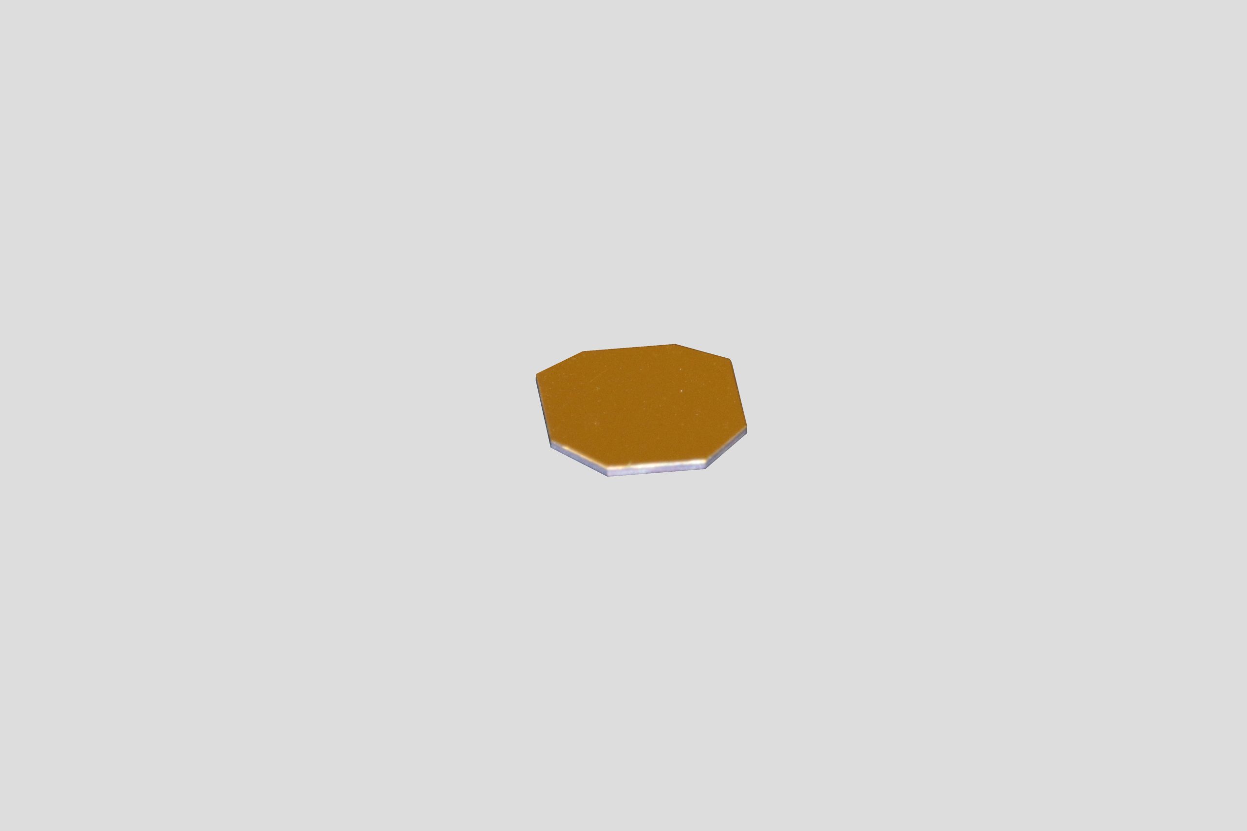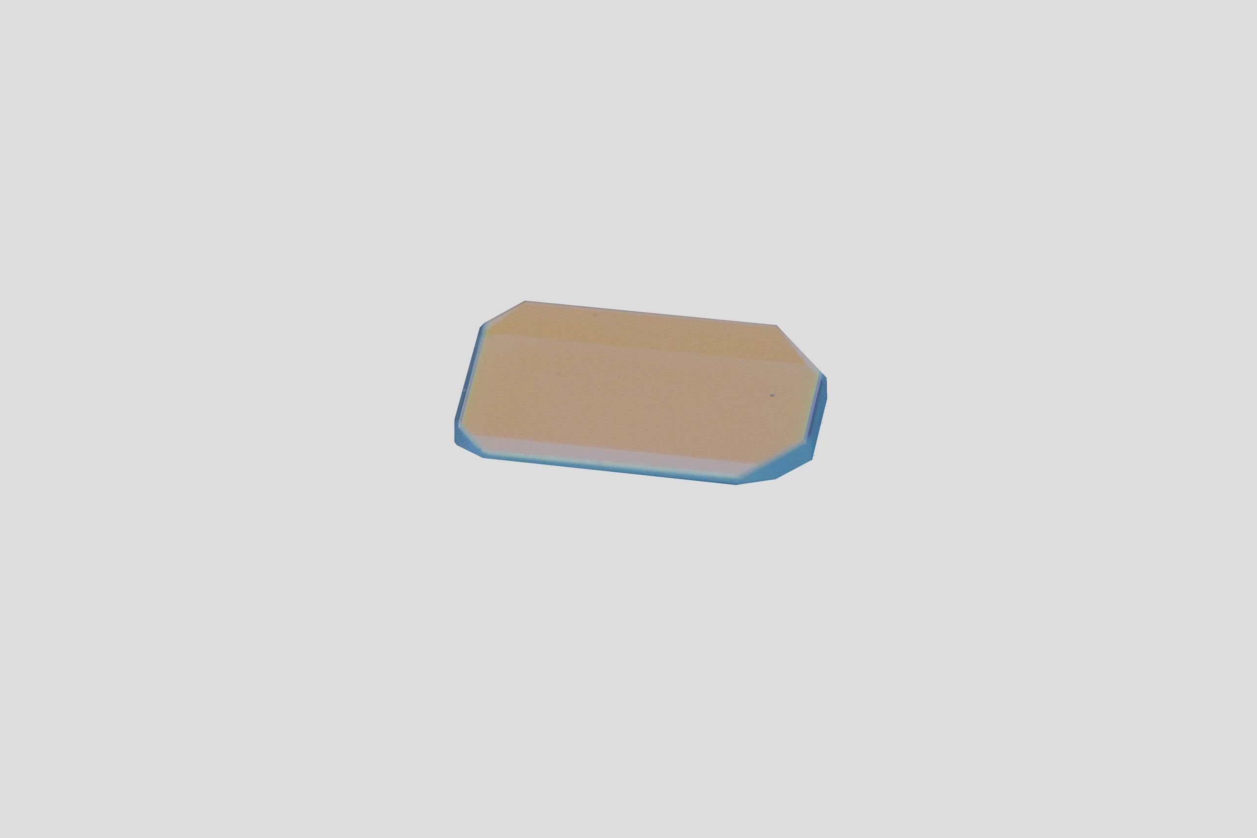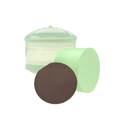
Product Description
Monocrystalline Si is produced by the following process: Quartz sand - metallurgical grade silicon - purification and refining - deposited polycrystalline silicon ingots - monocrystalline silicon - wafer cutting. The main application of monocrystalline Si is to be applied as the semiconductor materials and the field of solar energy and solar heating, etc.
Main Advantages:
Single inspection is available
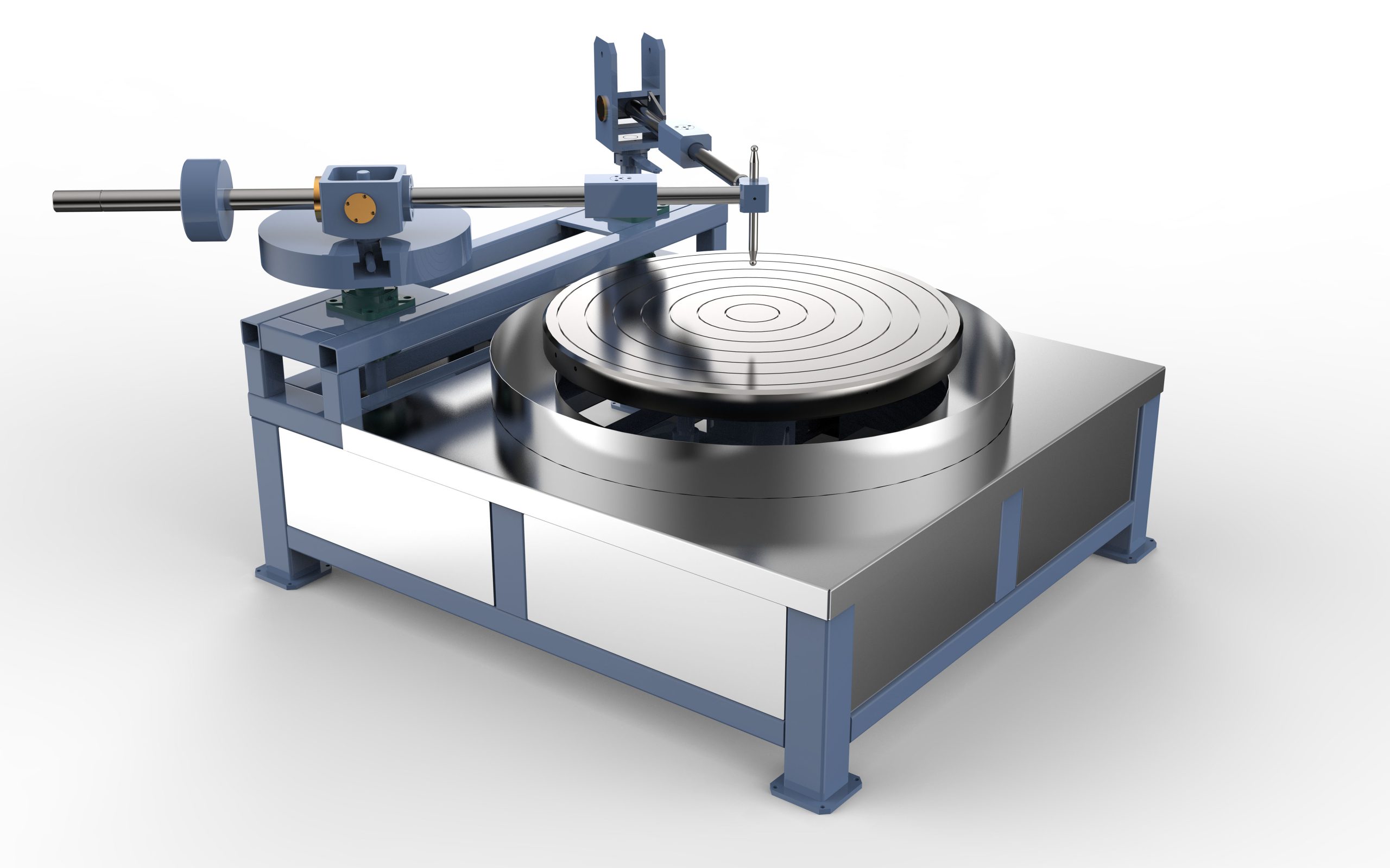
MCZ (Superconducting Magnetic Czochralski) growth method
Maximum diameter of 485mm
Zero dislocation defects
High growth yield
Impurity content is extremely low
Typical applications:
Semiconductor materials
Solar energy
Solar heating
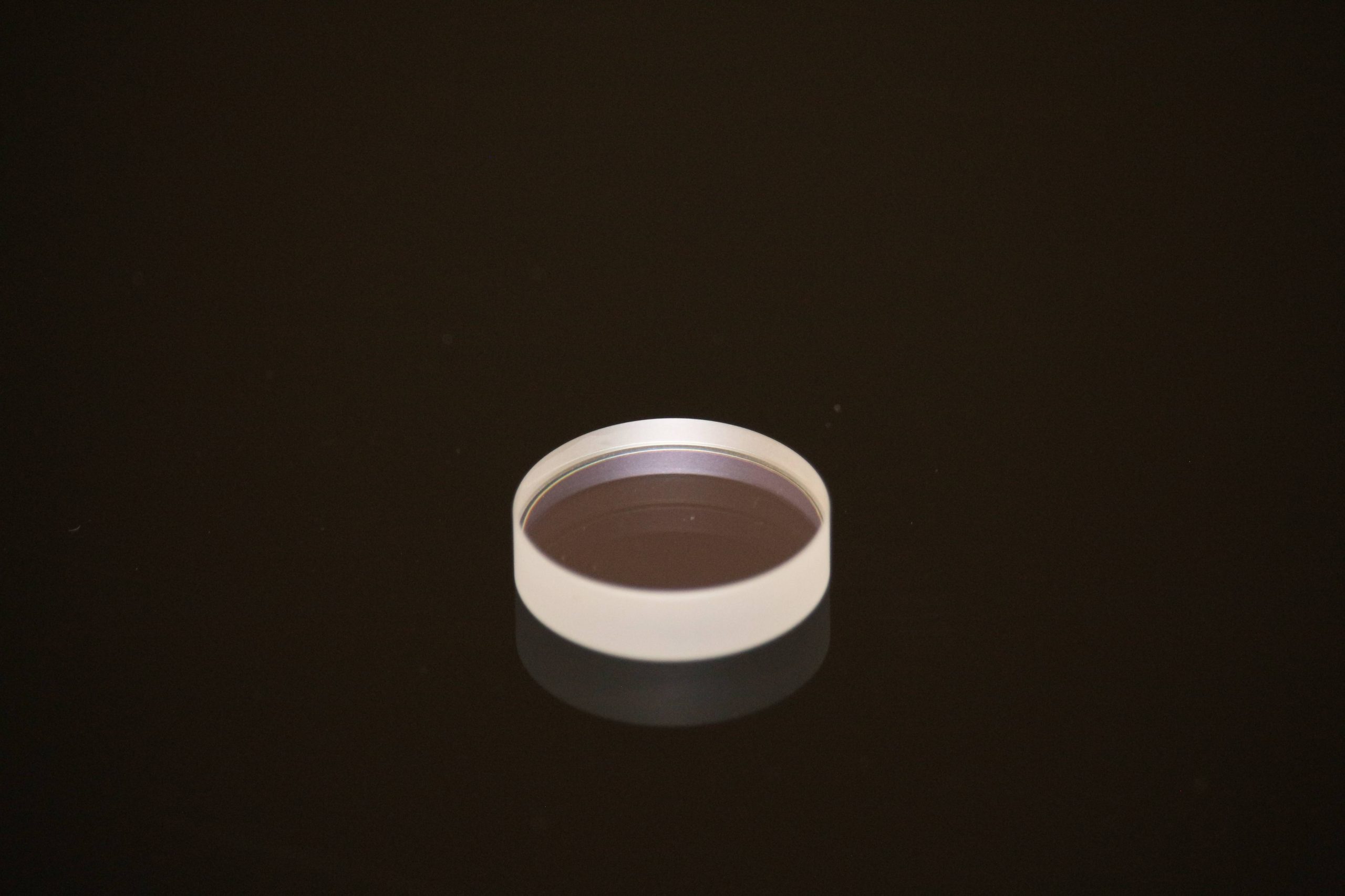
Material Properties
| Material | Si |
| Chemical Formula | Si |
| Density | 2.33g/cm³ |
| Purity | 99.999% |
| Dimension tolerance | ±0.1mm |
| Surface | 3.2Ra |
| Color | Light grey |
Grown by Czochralski method
Diameter: up to 485mm
Dopant B (Borum)
Type of conductivity: P
Orientation: 100
Resistivity: up to 10000
Notch-yes Notch Location: 110
Notch size: 2,3 mm
shape of the Notch: V
Wafer thickness: 775±25 microns Type of marking: laser Marking location Reverse side Edge Profile: SEMI T/4